
PRODUCT
PRODUCT
CONTACT US
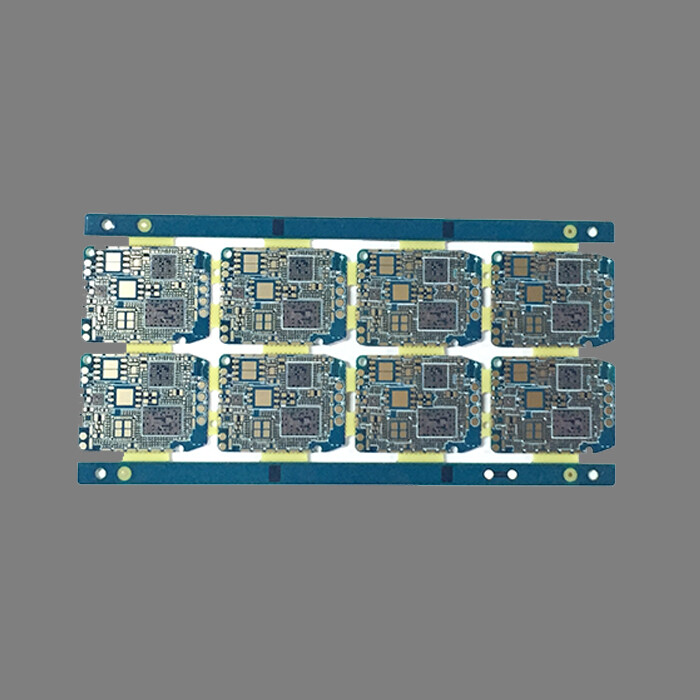
Commodity Name: Safety Control Printed Circuit Board
Brand Name: HFast
Layers: 6L
Board Thickness: 1.60mm
Minimum Hole Size: 0.20mm
Minimum Line Width: 0.13mm
Minimum Line Spacing: 0.13mm
Color: Blue Oil and White Legend
Surface Treatment: Gold Plating
Challenges and Development Trends of Safety Control PCB
1. Challenge:
*Balancing cost and performance/reliability: The market is price sensitive, but high quality requirements lead to cost pressures.
Miniaturization and High Density:Devices (especially IPC) pursue miniaturization and require higher density PCB design (HDI applications are increasing).
Heat dissipation bottleneck: AI chips, high-resolution sensors, and high-speed networks bring greater heat load, increasing the difficulty of heat dissipation design.
*Supply chain security: relies on critical chips (main SoC, AI NPU, high-end sensors).
*Security threat: The demand for hardware level security design (such as secure boot and encryption chip integration) has increased.
Diversity of standards:Meet safety regulations in different regions around the world EMC、 Wireless authentication requirements.
2.Development Trends:
*Deep integration of AI: Edge AI chips are popularized in IPC/NVR, promoting higher computing power, higher bandwidth, and more complex PCB designs.
Higher definition and intelligence:4K/8K, HDR, multispectral (visible light+thermal imaging) are popularized, and intelligent analysis functions are sinking.
*Wireless and Fusion: With the increasing application of wireless technologies such as WiFi 6/7, 5G RedCap, LoRa, PCB needs to integrate more RF modules.
PoE+Popularization:Higher power PoE meets the needs of smart ball cameras, panoramic cameras, and other equipment.
*Low power design: The increasing demand for battery powered IoT sensors is driving the ultimate low-power PCB technology.
*HDI technology application: Micro hole and blind buried hole technology are more commonly used in high-end compact devices.
Advanced heat dissipation solution: Uniform heat plates and small heat pipes integrated into PCB heat dissipation design.
*Hardware based network security: The integration of hardware security modules such as TPM and security SE has been improved.
*Sustainability: Halogen free materials, recyclable design, and improved energy efficiency.
Online Message
Application


CONTACT US
Please use the form below to get in touch.
If you need a reply we will get in touch as soon as possible.