
PRODUCT
PRODUCT
CONTACT US
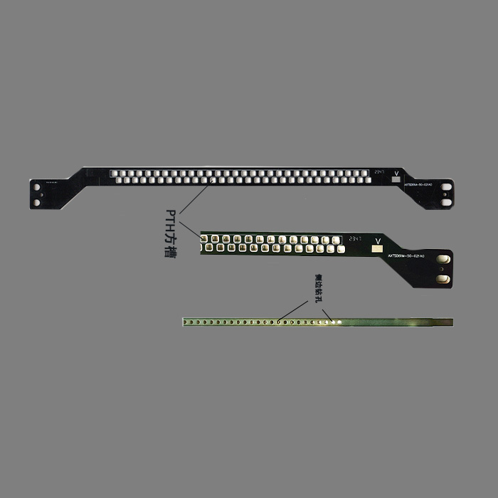
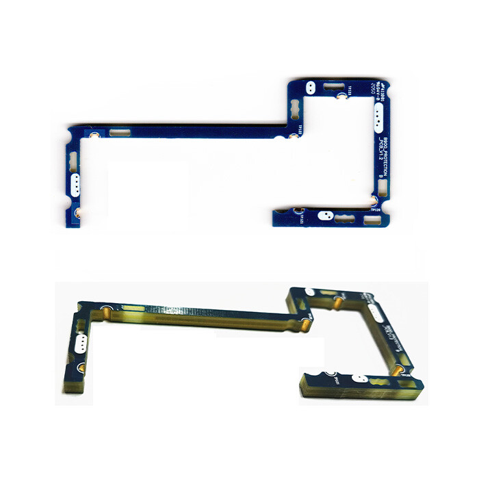
Commodity Name: Thick Printed Circuit Board for POS Machine
Brand Name: HFast
Layers: 6L
Board Thickness: 4.5mm
Minimum Hole Size: 0.50mm
Minimum Line Width: 0.127mm
Minimum Line Spacing: 0.127mm
Surface Treatment: Gold Plating
Color: Blue Oil and White Legend
Advantages: Thickness exceeds the norm, circuit board and can shipped out by PCS
Brief Introduction of Thick PCB
Thick PCB board "usually refers to a printed circuit board with a thickness significantly greater than the standard FR-4 PCB (usually 1.6mm). Their design, manufacturing, and application all have their unique features.
Thick PCB board is a solution that meets specific requirements such as high power, high mechanical strength, high reliability, special thermal management, or high voltage insulation. They break through the physical limitations of standard PCBs, but also bring significant manufacturing complexity and cost increases. Successfully designing and manufacturing thick plates requires a deep understanding of their application requirements, material properties, and process challenges, as well as full consideration of manufacturability during the design phase and close collaboration with experienced PCB manufacturers.
Definition and Standards of Thick PCB
1. * * Thickness range:**
*Standard thickness: The most common standard PCB thickness is 1.6mm.
*Definition of Thick Plate: PCB with a thickness of ≥ 2.0mm can be classified as "thick plate". In practical applications, the thickness range of thick plates is very wide, from * * 2.0mm to 8.0mm or even thicker * * (such as some backplates and power module substrates).
*Relative concept: "Thick" is also a relative concept. For PCBs with a large number of layers (such as 20 or more), even if the total thickness reaches 3.2mm or 4.0mm, the single-layer dielectric thickness may not be particularly thick, but the overall board thickness belongs to the category of thick plates. Sometimes it also refers to the fact that the core board itself is relatively thick (even if the total thickness is not particularly large).
2. * * Core materials:**
*Although FR-4 (epoxy resin glass cloth laminated board) is still the most commonly used substrate, thick plates have higher performance requirements for the material.
*Common materials:
** * Standard FR-4: * * Suitable for thick plates of general thickness.
*High Tg FR-4: Tg (glass transition temperature) is higher than the standard FR-4 (usually Tg>170 ° C or 180 ° C), providing better high-temperature stability and anti delamination ability, which is crucial for multi-layer lamination and reliability of thick plates.
*Special materials: For extremely high power or high-frequency applications, materials such as Rogers, polyimide, metal substrates (such as aluminum substrates), ceramic substrates, etc. may be used, and these materials themselves or their structures may result in thicker final PCBs.
Main Application Scenarios of Thick PCB (why thick plates are needed?)
Main application scenarios (why thick plates are needed?)
1. * * High power/high current applications:**
** * Power converter/inverter: * * Requires high current carrying capacity, thick plates allow the use of thicker copper foils (such as 2oz, 3oz, or even 6oz or more) * * to reduce wire resistance, reduce heat generation, and improve current carrying capacity.
*Motor driver: It also needs to handle high currents and possible high voltages.
*Power distribution system: such as busbars or high current PCBs in distribution panels, industrial control cabinets.
*High power LED lighting: Heat dissipation and current carrying are key factors.
2. * * High mechanical strength and stability requirements:**
*Industrial equipment/automation: PCBs need to withstand vibration, impact, or significant mechanical stress.
*Aerospace and Defense: The requirements for reliability and stability in harsh environments are extremely high.
*Heavy duty connectors/backboards: The connector area needs to withstand the mechanical force of repeated insertion and extraction, and thick plates provide better support and prevent deformation.
** * Large or heavy components: * * Support heavy components such as transformers, heat sinks, electrolytic capacitors, etc., to prevent board bending or solder joint cracking.
3. * * Thermal management:**
*Thick plates themselves have a larger heat capacity, which helps to absorb and evenly distribute heat (although their thermal conductivity may not be high).
*Provided space for embedded heat dissipation copper blocks/flat surfaces, connected to the board surface or external heat sink through thermal vias.
*Combined with a thick copper layer, heat can be more effectively conducted away from heating elements such as power MOSFETs and diodes.
4. High voltage applications:**
*It is necessary to ensure sufficient creepage distance and electrical clearance. Thick plates allow for the installation of thicker insulation layers between different layers or between different networks on the same layer to meet high-voltage insulation requirements (such as industrial control, medical, X-ray equipment).
5. * * Complex multi-layer interconnect structure:**
*A multi-layer PCB (such as 20 or more layers) stacked together will naturally be very thick.
*Special processes such as buried resistance and buried capacitance may be required, which increases the interlayer structure and thickness.
*Used as a system backplane, it carries a large number of high-speed connectors and signal channels, requiring high-density wiring and structural strength.
6. RF/Microwave Applications (Specific Situations):**
*Some RF structures, such as thicker microstrip lines, require a specific thickness of dielectric layer to achieve the target impedance.
*Thick substrates are sometimes used to reduce losses or meet specific mechanical requirements.
Design and Manufacturing Characteristics of Thick PCB Boards (Challenges and Precautions)
Design and Manufacturing Characteristics of Thick PCB Boards (Challenges and Precautions)
1. * * laminating process challenge:**
*Uniformity of Pressure and Temperature: During the compression process of thick plates, it is more difficult for heat and pressure to be evenly transferred to the central layer of the core plate, which can easily lead to problems such as delamination, uneven resin curing, and misalignment between layers. More precise presses and optimized pressing programs (such as multi-stage heating/pressurization) are needed.
*Material selection: High Tg, high reliability, and low CTE (coefficient of thermal expansion) materials must be selected to withstand compression stress and subsequent working environment stress, preventing delamination and plate bursting.
** * Glue flow control: * * Control the flowability of the resin in the semi cured sheet to prevent excessive glue flow from causing local missing glue or uneven thickness.
2. * * Drilling Challenge:**
*Hole wall quality: When drilling deep holes, it is easy to encounter problems such as drilling deviation, rough hole walls, nail heads, and resin stains. High performance drilling rigs, special drill bits (such as segmented drills, hard alloy drill bits), optimized drilling parameters (speed, feed rate, tool return speed), and frequent replacement of drill bits are required.
*Depth to aperture ratio: Thick plates typically have a larger aspect ratio. A standard aspect ratio (plate thickness/aperture) of around 10:1 is generally considered a challenge, while thick plates may reach 15:1 or even 20:1. High aspect ratio holes pose significant challenges to drilling and hole metallization.
** * Removal of drilling debris: * * Thoroughly removing drilling resin grease in deep holes is crucial for the reliability of hole metallization, and requires more powerful drilling debris removal processes (such as plasma slag removal).
3. * * Hole metallization challenge:**
*Uniformity of Electroplating: It is very difficult to achieve a uniform copper coating in deep holes. The middle of the hole is prone to thinning, leading to an increase in hole resistance or even an open circuit. Special electroplating equipment (such as pulse electroplating, horizontal electroplating line), electroplating solution formula, and process control are required.
*Reliability: Ensure good adhesion between the copper layer on the hole wall and the dielectric material, avoiding cracking under thermal stress (such as welding, environmental temperature changes) (known as "pull-out failure").
4. * * Outer layer circuit production:**
*Etching uniformity: For boards using ultra thick outer copper foil, it is necessary to ensure that the side walls of the lines are steep during etching to avoid excessive or insufficient etching. Multiple etching or special etching agents may be required.
*Thin line capability: The thick copper layer limits the ability to etch fine lines.
5. * * Thermal stress management:**
*During welding (especially wave soldering) of thick plates, due to their high heat capacity, heating and cooling are slow, resulting in greater thermal stress. It is necessary to optimize the welding curve to prevent board deformation or damage to components, solder joints, and copper holes due to thermal stress.
*The CTE matching problem of the board itself may be more significant on thick plates.
Key considerations for designing thick PCB of Thick PCB
1. * * Clarify requirements: * * First, clarify whether * * requires thick copper * *, * * requires thick dielectric layer * *, or * * requires overall structural strength * *? This will guide material selection and stacking design.
2. Material selection: Strictly select substrates and semi cured sheets with high Tg, high reliability, low CTE, suitable for thick plate lamination. Consider the type of copper foil (rolled copper may have better ductility than electrolytic copper) and thickness.
3. * * Stacked design:**
*Symmetry: The central layer should be as symmetrical as possible in terms of material type, thickness, and copper layer distribution to minimize warping.
*Copper balance: The copper area of adjacent layers should be balanced as much as possible.
** * Core board selection: * * Thicker core boards may be required to reduce the number of lamination layers.
4. * * Aperture and ring design:**
** * Avoid extremely small holes: * * Use larger apertures as much as possible to reduce the aspect ratio (for example, for a plate thickness of 3.2mm, the minimum aperture is recommended to be ≥ 0.3mm, and the aspect ratio is approximately 10.7).
** * Increase the hole ring: * * Provide more drilling tolerance space and better connection reliability.
5. * * Thermal design:**
*Fully utilize the inner copper plane for heat dissipation.
*Reasonably design the heat dissipation hole array.
*Consider embedding special heat dissipation structures such as copper blocks.
*Pay attention to component layout and heat dissipation path.
6. * * Mechanical design:**
*Consider supporting points and fixing hole positions.
*Avoid placing vulnerable components or fine wires in stress concentration areas (such as near large connectors).
*Communicate with structural engineers about installation and stress conditions.
7. DFM: * * Communicate closely with PCB manufacturers on design details to ensure that the design meets their thick plate process capabilities and requirements. Conduct a manufacturing feasibility review as early as possible.
Online Message
Application


CONTACT US
Please use the form below to get in touch.
If you need a reply we will get in touch as soon as possible.