
PRODUCT
PRODUCT
CONTACT US
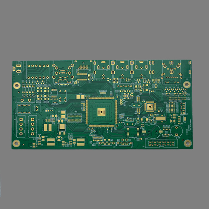
Key Parameters of Safety Control PWB
Commodity Name: Safety Monitoring Camera Control Printed Circuit Board
Brand Name: HFast
Layers: 4L
Board Thickness: 1.60mm
Minimum Hole Size: 0.20mm
Minimum Line Width: 0.13mm
Minimum Line Spacing: 0.13mm
Color: Green Oil and White Legend
Surface Treatment: Gold Plating
Brief Introduction of Safety Control PCB
The Safety PCB can also be called as the security PCB board is the core hardware cornerstone for building modern security and prevention systems. They carry key functions such as video capture, image processing, signal transmission, intelligent analysis, alarm linkage, access control, power management, and network communication. They are indispensable "brains" and "neural networks" for security equipment such as cameras (IPC), network video recorders (NVR), digital video recorders (DVR), access controllers, alarm hosts, and video intercoms.
Characteristics of Safety PCB
1. High reliability and stability design;
2. Adaptability to harsh environments;
3. Precision manufacturing and process requirements;
4. Safety and compliance features;
5. High precision wiring;
6. Wide temperature range and material stability;
7. Intelligence and high-speed interconnection.
Key components and technical characteristics of security PCB
1. Core PCB type:
*Network camera board:
*Image sensor board:Connected to CMOS/CCD sensors, including analog front-end circuits.
Main control board:Integrated main SoC (including ISP, encoder), DDR memory, flash memory, network PHY, audio codec, interface controller, etc. It is the core of IPC.
Motor drive board:Control pan tilt, zoom, and aperture (PTZ camera).
*Infrared light board: Control the IR LED and its driving circuit (night vision function).
Power Supply and PoE Board:Handling power input/PoE power supply and conversion.
*NVR/DVR motherboard: Core processing platform, integrated with high-performance multi-core CPU, large capacity DDR, video decoding/output chip, multiple SATA/NVMe interfaces, gigabit/ten gigabit network ports, expansion slots, etc. High complexity and multiple layers (6-12 layers).
*Access control board: Processing card reader (IC card, fingerprint, face) signals, controlling electric locks, managing access control logic, and networking communication. High reliability and real-time performance are required.
*Alarm motherboard: Receive and process signals from various detectors (infrared, door magnets, smoke detectors, gas detectors), trigger alarm outputs, and communicate.
*Visual intercom indoor/door panel: Integrated audio and video processing, encoding and decoding, display driver, network communication, and control logic.
2. Key material selection:
Substrate:
High Tg FR-4:Absolute mainstream. Choose Tg ≥ 150 C (preferably 170C) low CTE high CAF resistance low loss (for high-speed parts) , halogen-free materials. Such as Isola FR408HR, Panasonic Megtron 4/6, Shengyi S1000/1150G, ITEQ IT-180A, etc. Meet long-term reliability and environmental requirements.
Metal substrate:Used for high-power local heat dissipation (such as infrared lamp drivers, high-power PoE interfaces).
*Copper foil:
Standard 1oz: Used for most signal layers.
*Thick copper (2oz):Used for high current paths (power input, PoE, motor drive, infrared drive).
*Solder mask: High heat resistance, high adhesion, excellent chemical resistance, and good insulation are required. Commonly used green or black (to reduce glare interference). Matte surface may be required to reduce light reflection.
*Surface treatment:
Nickel immersion gold:Mainstream choice. Providing a flat welding surface, excellent weldability, oxidation resistance, and long-term reliability, suitable for fine pitch BGA and multiple soldering. The gold layer is advantageous for weak signal connections (such as sensors).
Tin deposition:Low cost, good solderability. Assess the risk of tin whiskers and their performance under high temperature and humidity conditions.
*OSP: The lowest cost, used for low-end, short production cycle, and simple soldering boards. Poor protection.
*Silver deposition: The signal performance is good (especially at high frequencies), but it is prone to oxidation and sulfurization. It should be used with caution in sulfur-containing environments or scenarios with high long-term reliability requirements.
*Electroplated hard gold: Used for gold fingers (such as memory slots, expansion card slots).
3. Design points:
Layout partition:
Physical isolation: Strictly separate analog (video input, audio input/output), digital (main control, DDR), high-frequency (wireless module, clock), and power (power supply, motor drive, PoE) areas. Slot if necessary.
Sensitive circuit protection: The front end of the image sensor, clock circuit, and reset circuit should be kept away from noise sources and shielded or grounded.
High speed signal design:
Impedance control: for DDR memory bus, MIPI CSI/DSI (sensor/screen interface) HDMI、USB3.x、 Accurate impedance control (90 Ω/100 Ω differential) using high-speed Ethernet and other differential pairs.
The DDR data line group with equal length wiring strictly follows the same length, and the clock and data/address lines meet the timing requirements.
Minimize crosstalk: Maintain line spacing, avoid long-distance parallel wiring for high-speed signals, and use ground isolation.
Optimize via: reduce the number of high-speed path via holes, optimize via structure (reverse solder pad), and consider back drilling for key high-speed via holes.
Power integrity:
Advantages of multi-layer boards: Utilizing power layers and geological layers to construct low impedance PDNs.
Decoupling capacitor strategy: Arrange decoupling capacitors of different capacitance values and types (including high-frequency ceramic capacitors) near the chip power pins.
High current path: Short and wide (thick copper) power supply wiring to reduce voltage drop and heat generation.
Thermal management:
Heat dissipation pads: Large exposed copper pads are designed below the main SoC, network chip, and power chip to connect internal layers for heat dissipation.
Thermal conductive via array: densely drill holes under the heating element and fill them with thermal conductive material to conduct heat to the back of the PCB or heat sink.
Layout optimization: Disperse heat sources and avoid stacking.
*External heat dissipation: relies on heat sinks, heat pipes, and fans (especially NVR/IPC boxes).
*EMC design:
Filtering:Add filtering components to all power inlet, signal line interface, and external connection cable inlet.
Shielding:Use metal shielding covers in critical areas (pay attention to the design of heat dissipation holes).
*Grounding via array: Dense grounding vias are arranged around the edges of the PCB, interfaces, and high-speed signal lines.
*Lightning protection and surge protection: Outdoor equipment interfaces (network, power, video, alarm IO) must integrate multi-level protection circuits such as TVS/MOV/GDT, with a wide and short discharge path and isolation from sensitive circuits.
DFM/DFT: Consider manufacture ability (avoid process difficulties) and reserve testing points (ICT, functional testing).
Online Message
Application


CONTACT US
Please use the form below to get in touch.
If you need a reply we will get in touch as soon as possible.