
PRODUCT
PRODUCT
CONTACT US
The core mission of medical electronic PCB: the physical cornerstone of life protection
They are the "hearts" and "nerves" of medical electronic products such as implantable devices (such as pacemakers), life support systems (such as ventilators, dialysis machines), diagnostic devices (such as CT, MRI, ultrasound), therapeutic devices (such as laser surgical knives, defibrillators), in vitro diagnostic devices (such as blood glucose meters, gene sequencers), and wearable health monitoring devices (such as electrocardiogram patches).
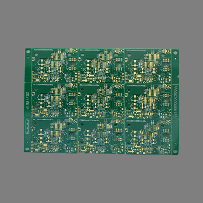
Key Parameters of Medical Blood Pressure Monitor PCB
Commodity Name: Thermometer Printed Circuit Board
Brand Name: HFast
Layers: 2L
Board Thickness: 1.60mm
Minimum Hole Size: 0.30mm
Minimum Line Width: 0.25mm
Minimum Line Spacing: 0.25mm
Color: Green Oil and White Legend
Surface: Gold Plating
Key technical characteristics of Medical PCB
1. Material selection:
*Substrate:
High reliability FR-4:is the most commonly used, choosing high Tg low CTE, low moisture absorption,CAF resistance halogen-free grade (meeting environmental and safety requirements). Ensure that the material meets UL 94 V-0 flame retardant rating.
*Polyimide: Used for applications that require extremely high heat resistance, excellent dimensional stability, and flexibility, such as wearable devices, flexible sensors, and internal connections in implanted devices.
*Ceramic substrate: Used in applications that require excellent thermal conductivity, high-frequency performance, or ultra-high reliability, such as high-power laser modules and certain sensors.
Special substrate:Implantable devices may use biocompatible laminates or use special packaging * * (such as titanium alloy, ceramic, Parylene coating).
*Copper foil: Standard or low profile copper foil is usually used. Thick copper is used for the power supply section.
*Solder mask: requires high adhesion chemical resistance (disinfectant resistance), heat resistance (multiple welding and sterilization resistance), biocompatibility(contact parts), excellent insulation * *. The color is mostly green, but there are also white (for easy observation of cleanliness) and black (to reduce glare interference).
*Surface treatment:
*Nickel immersion gold: The most mainstream choice. Good flatness, excellent solderability, low and stable contact resistance, excellent corrosion resistance, suitable for fine pitch components (BGA, QFN) and multiple soldering. The gold layer provides a biologically inert barrier (key!).
Sinking silver: Good weldability and low cost. But it is prone to oxidation and sulfurization, and its long-term reliability (especially in sulfur-containing disinfection environments) is not as good as ENIG, so careful evaluation is needed.
*Electroplated hard gold: Used for connector contacts (gold fingers) with high insertion and extraction times, wear-resistant.
*OSP/Tin Deposition: It may have applications in low-cost medical equipment that is non critical and non-contact, but its long-term reliability and disinfection resistance need to be rigorously evaluated.
Special coating: Implanted devices or contact points may require additional biocompatible coatings (such as Parylene, medical grade silicone).
2. Design and Layout Routing:
Safety isolation design:Clearly divide the high voltage area, low voltage area, and patient contact area, strictly comply with the requirements of creepage distance and electrical clearance, and cut slots if necessary.
*Low noise design:
*Partition: Strictly separate analog (especially weak signals), digital, power, and RF circuits.
*Grounding: Carefully designed low impedance, low-noise grounding system (commonly star grounding or mixed grounding) to avoid ground loops. Reasonable segmentation and connection of analog ground, digital ground, and shell ground.
Shielding:Use shielding covers, grounding, and Faraday cages for sensitive circuits (preamplifiers).
Wiring: Short and straight signal path, avoiding sharp angles, sensitive signal lines are routed through the inner layer (strip line), using differential signal transmission.
*Power integrity: The multi-layer board provides a complete power/ground plane and extensively uses decoupling/bypass capacitors.
Design for manufacturability and testability:Consider production yield and reserve sufficient testing points (flying pin testing, ICT testing, functional testing).
Thermal management:Reasonably layout heating elements, use heat dissipation holes, heat dissipation pads or metal substrates to dissipate heat, and avoid local overheating affecting the lifespan and measurement accuracy of components.
3. Manufacturing and Quality Control:
*Clean production environment: Some high demand PCBs (such as implantable ones) need to be produced in a highly clean environment to control particle pollution.
*Strict process control: All parameters (drilling, etching, lamination, electroplating, solder mask, surface treatment) need to be precisely controlled with high tolerance requirements.
100% electrical testing: Flying needle testing or needle bed testing is standard.
*Automated optical inspection: AOI checks for welding defects, component errors, omissions, and screen printing issues.
*X-ray inspection: Used to inspect hidden solder joints and internal structures such as BGA and QFN.
*Micro slice analysis: Spot check or slice the failed board to inspect the microstructure such as hole copper thickness, interlayer bonding, and solder joint quality.
** * Reliability testing: * * may include temperature cycling, high temperature and high humidity aging, vibration testing, etc., especially for implantable and critical devices.
*Cleanliness and ion contamination testing: Ensure that residual ion pollutants (such as soldering flux) are below strict standards (such as ROSE Test) to prevent electrochemical migration (CAF) and corrosion.
*Complete documentation and traceability: All materials, processes, and testing data must be fully recorded and archived for many years.
Online Message
Application


CONTACT US
Please use the form below to get in touch.
If you need a reply we will get in touch as soon as possible.