
PRODUCT
PRODUCT
CONTACT US
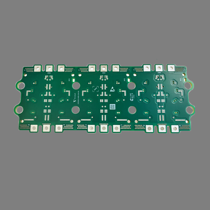
Commodity Name: Portable Power Bank Inverter Printed Circuit Board
Brand Name: HFast
Layers: 2L
Board Thickness: 1.60mm
Copper Thickness: 2.5oz
Minimum Hole Size: 0.40mm
Minimum Line Width: 0.30mm
Minimum Line Spacing: 0.30mm
Color: Green Oil and White Legend
Surface Treatment: Lead Free HASL
Challenges and Development Trends of Energy Storage PWB
1.Challenge:
*Balancing cost and high performance/reliability: * * Strict requirements result in significantly higher costs than ordinary industrial PCBs.
*High precision and strong interference coexist: Achieving uV/mV level precision sampling in harsh EMI environments is a huge challenge.
*The safety pressure is enormous: Any design flaw can lead to serious safety accidents, and the responsibility is significant.
Thermal management challenge: High current and high-density packaging bring heat dissipation challenges.
*Rapid evolution of standards and regulations: It is necessary to continuously track and meet the constantly updated safety, performance, and environmental standards around the world.
*Supply chain stability: Strong dependence on the supply chain of key components such as high-precision AFEs, isolation devices, and automotive grade MCUs.
2. Development Trends:
Higher integration:
AFE chip integration improvement:Single chip supports more channels, higher precision, and integrated balanced drivers.
Modular design: Using standardized BMS daughter boards (such as individual acquisition+equalization modules) for easy maintenance and expansion.
*SIP/SoC application: Integrating MCU, AFE, isolation, communication and other functions into fewer chips or packages.
Smarter BMS algorithm:Supports more accurate SoX estimation, status diagnosis, predictive maintenance, and places higher demands on hardware platforms.
Functional safety:Hardware design that complies with ASIL level (ISO 26262) or SIL level (IEC 61508) becomes standard for high-end systems.
*Wireless BMS: Explore the use of wireless communication (such as Bluetooth Mesh) to replace some wired communication, simplify wiring, and improve flexibility (reliability, real-time performance, and power consumption challenges still need to be addressed).
*Advanced Sensor Integration: Integrate more sensors to monitor the internal state of the battery, such as pressure and gas.
*Higher voltage platform: Developing towards 1500V DC and above, higher requirements are placed on isolation and safety design.
*Liquid cooling is widely used in high-power systems, and PCB design needs to consider compatibility with the cold plate and thermal interface.
*Sustainability: Using environmentally friendly materials to improve energy efficiency (reduce self power consumption).
Online Message
Application


CONTACT US
Please use the form below to get in touch.
If you need a reply we will get in touch as soon as possible.