
PRODUCT
PRODUCT
CONTACT US
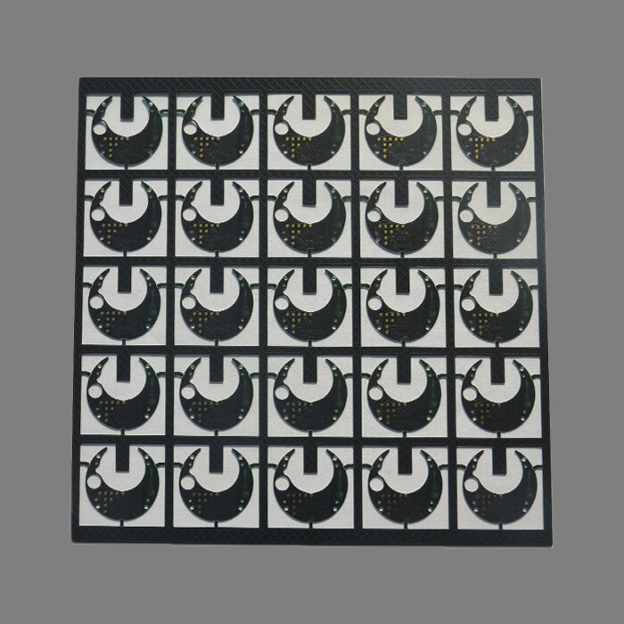
Commodity Name: Digit Robert Computer Printed Circuit Board
Brand Name: HFast
Layers: 2L
Board Thickness: 1.00mm
Minimum Hole Size: 0.25mm
Minimum Line Width: 0.10mm
Minimum Line Spacing: 0.10mm
Oil Color: Green Top and Black Base
Surface Treatment: Gold Plating
Advantages: Solder Mask Ink with Two Colors in Two Sides
Key characteristics and technical challenges of computer PCB boards
1. Extremely high complexity and number of layers:
*Multi layer structure: Modern mainstream motherboards generally adopt 6-layer and 8-layer designs, while high-end desktop motherboards, workstation motherboards, and server motherboards can reach 10, 12, or even more layers. The number of layers is used for:
*Provide a complete power layer and geological layer (reduce impedance, shield interference).
*Can accommodate dense signal wiring, especially high-speed differential pairs.
*Implement a complex power distribution network.
High density wiring:Component pins are densely packed (especially BGA packaging for CPUs and chipsets), requiring a large number of signal lines to be laid in limited space, with increasingly fine line widths/spacing (usually starting at 4mil/4mil, and finer for high-end boards).
2.Ultimate high-speed signal integrity:
*High frequency challenge: CPU and memory (DDR4/DDR5), CPU and PCIe devices (PCIe 4.0/5.0/6.0), extremely high data transfer rates (up to tens of Gbps) between CPU and chipset, operating at GHz level.
Key requirements:
*Accurate impedance control: High speed differential pairs (such as PCIe, USB 3. x, SATA, DDR clock/data lines) must strictly match the design impedance (usually 90 Ω or 100 Ω differential).
*Minimize losses: Use PCB substrates with low loss or very low loss (such as high-performance FR-4 models like Isola FR408HR, Panasonic Megtron 4/6/7/8, Taiguang EM series, etc.), especially on critical high-speed channels.
Reduce crosstalk:Adequate spacing should be maintained between adjacent signal lines, or ground wire isolation (grounding) should be used.
Control reflection:Avoid sudden changes in wiring impedance (such as via holes and corners), optimize via design (back drilled stub).
*Equal length wiring: For parallel buses (such as DDR memory channels) and differential pairs, strict equal length wiring is required to meet timing requirements.
3. Powerful power delivery system:
*High current demand: Modern high-performance CPUs and GPUs have huge power consumption (up to several hundred watts), requiring extremely stable high current power supply.
*VRM design:**
*Multiphase power supply: A multi-phase parallel circuit composed of PWM controller, DrMOS (or separate Driver+MOSFET), inductor, and filtering capacitor, which shares the current, reduces the thermal load of each phase, and improves efficiency and response speed. The number of VRM phases on high-end motherboards can reach 16 or more.
*High quality components: Use low internal resistance MOSFETs, high saturation current inductors, and low ESR solid-state capacitors.
*PCB design: The power layer uses thick copper (2oz or above) to optimize the current path, reduce impedance and heat generation. Heat dissipation design is crucial (heat sink, heat pipe connection).
*Power integrity: Ensure minimal voltage ripple and fast transient response to avoid system instability caused by voltage fluctuations.
4.Strict electromagnetic compatibility:
*Multiple sources of self interference: High speed digital signals and switching power supplies are strong sources of interference.
*Design Strategy:
*Partition Layout: Physically isolate analog (audio), digital, high-speed, and high-power areas.
Complete reference plane: The multi-layer board provides a continuous ground plane and power plane (try not to divide).
** * Shielding: * * Use metal shielding covers in critical areas such as M.2 SSD interfaces and WiFi modules.
Filtering:Add filtering circuits (magnetic beads, common mode inductors, TVS tubes) at the power inlet and interface (USB, Ethernet port).
*Grounding via array: A large number of grounding vias are drilled around the edges of the PCB and critical signals to form a "Faraday cage" effect and suppress edge radiation.
5. Thermal management:
Large fever generator:VRM, CPU power supply area, chipset M.2 SSD、 High speed network chips are the main heat sources.
*PCB heat dissipation design:
Heat dissipation pad:A large exposed copper pad is designed at the bottom of the heating chip to connect the internal ground layer for heat dissipation.
Thermal conductive via: * * Dense holes are drilled below the heating element and filled with thermal conductive material to conduct heat to the back or internal ground layer of the PCB.
*Layout optimization: Avoid stacking heating elements together.
*External heat dissipation: relies on heat sinks (aluminum/copper), heat pipes, fans, and chassis air ducts for final heat dissipation.
6. Scalability and Interface:
*Diversified slots and interfaces: Provides PCIe x16 (graphics card), PCIe x1/x4 (expansion card), M.2 (NVMe SSD), SATA (hard drive/SSD), memory slots (DIMM/SODIMM), USB pins, fan interfaces, front panel interfaces, etc.
*Wiring Challenge: Ensure signal quality for each interface, especially for high-speed interfaces (PCIe, M.2, USB 3.0).
Online Message
Application


CONTACT US
Please use the form below to get in touch.
If you need a reply we will get in touch as soon as possible.