
PRODUCT
PRODUCT
CONTACT US
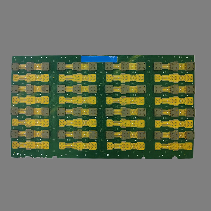
Key Parameters of Huawei 5G Antenna PCBA
Commodity Name: Huawei 5G Antenna Communication Printed Circuit Board Assembling
Brand Name: HFast
Layers: 2L
Board Thickness: 1.60mm
Minimum Hole Size: 0.20mm
Minimum Line Width: 0.25mm
Minimum Line Spacing: 0.25mm
Color: Green Oil and White Legend
Surface Treatment: Gold Plating
Advantages: High Frequency Material with Low DK
SMT/PCBA Introduction

The core challenge of communication PCB: the limits of speed and accuracy PCB
Unlike consumer electronics or ordinary industrial PCBs, communication PCBs face severe challenges brought by the continuous increase in signal speed (towards 100Gbps, 400Gbps or even higher) and frequency (millimeter wave frequency band):
1. High frequency signal integrity:**
Low loss:Signal transmission in a medium will result in loss (conductor loss+dielectric loss). At high frequencies (especially above GHz), dielectric loss becomes dominant. Require the use of * * ultra-low loss * * substrate material.
*Stable dielectric constant: The dielectric constant of the material must be highly stable (with minimal changes in frequency and temperature) to ensure precise impedance control and signal propagation speed.
*Accurate impedance control: High speed differential signals (such as SerDes channels) require strict impedance matching (usually 50 Ω single ended, 100 Ω differential). PCB design requires precise calculation and control of line width, line spacing, dielectric thickness, copper foil roughness, etc.
*Minimize signal distortion: Strictly control dispersion (different frequency components have different propagation speeds), attenuation, and jitter.
2. High speed digital signal integrity:
Extremely low bit error rate:High speed data links (such as 100G/400G Ethernet) require extremely low bit error rates. PCB design must minimize reflection crosstalk ground bounce noise .
*Power integrity: High speed chips have high instantaneous currents and require extremely low power distribution network impedance to reduce synchronous switching noise. Multi layer boards are required to provide a complete power/ground plane, and decoupling capacitors (including high-frequency ceramic capacitors and distributed capacitors) are extensively used.
** * Timing control: * * For parallel bus or clock allocation, precise control of routing length (equal length wiring) and propagation delay is required.
3. Electromagnetic compatibility:
Self EMI control:High speed signals are strong sources of interference and need to be suppressed through good shielding (shielding covers, grounding via walls), wiring strategies (avoiding sharp angles, grounding), filtering, and other means to suppress radiation.
*Anti external interference: The equipment needs to work stably in complex electromagnetic environments, and the design needs to consider anti-interference capabilities.
*EMC within the system: Effective isolation is required between different functional modules (digital, analog, RF, power) within the board to prevent mutual interference.
4. High density interconnection:
Component miniaturization:Chip packaging is developing towards BGA (Ball Grid Array), CSP (Chip Level Packaging), and QFN (Square Flat No Pin), with increasingly smaller pin spacing (<0.5mm).
*Multilayer: Complex communication devices commonly use PCBs with 12, 20, or even more layers.
*HDI technology: High density interconnect technology is the core, widely used in micro holes, blind holes, buried holes, disk holes, and finer line widths/spacing (as low as 3mil/3mil or even smaller).
5. Thermal management:
*High speed chips (CPU, FPGA, ASIC, optical module DSP/Driver) and RF power amplifier devices have huge power consumption and concentrated heat generation.
*PCB requires effective thermal conductivity and heat dissipation. Common methods include large copper sheets, heat dissipation via arrays, embedded copper blocks, metal substrates (such as aluminum substrates), and integrated heat pipes/heat exchangers.
6. High reliability:
*Communication equipment (especially backbone networks and base stations) require 24/7 uninterrupted operation, and failures may result in widespread service interruptions.
*PCBs need to have a long lifespan, high stability, and be able to withstand a certain degree of environmental factors such as temperature changes and humidity.
Online Message
Application


CONTACT US
Please use the form below to get in touch.
If you need a reply we will get in touch as soon as possible.